CVD SiC coating is reshaping the limits of semiconductor manufacturing processes at an astonishing rate. This seemingly simple coating technology has become a key solution to the three core challenges of particle contamination, high-temperature corrosion and plasma erosion in chip manufacturing. The world’s top semiconductor equipment manufacturers have listed it as a standard technology for next-generation equipment. So, what makes this coating the “invisible armor” of chip manufacturing? This article will deeply analyze its technical principles, core applications and cutting-edge breakthroughs.
Ⅰ. Definition of CVD SiC coating
CVD SiC coating refers to a protective layer of silicon carbide (SiC) deposited on a substrate by a chemical vapor deposition (CVD) process. Silicon carbide is a compound of silicon and carbon, known for its excellent hardness, high thermal conductivity, chemical inertness and high temperature resistance. CVD technology can form a high-purity, dense and uniform thickness SiC layer, and can be highly conformal to complex geometries. This makes CVD SiC coatings very suitable for demanding applications that cannot be met by traditional bulk materials or other coating methods.
Ⅱ. CVD process principle
Chemical vapor deposition (CVD) is a versatile manufacturing method used to produce high-quality, high-performance solid materials. The core principle of CVD involves the reaction of gaseous precursors on the surface of a heated substrate to form a solid coating.
Here is a simplified breakdown of the SiC CVD process:
CVD process principle diagram
1. Precursor introduction: Gaseous precursors, typically silicon-containing gases (e.g., methyltrichlorosilane – MTS, or silane – SiH₄) and carbon-containing gases (e.g., propane – C₃H₈), are introduced into the reaction chamber.
2. Gas delivery: These precursor gases flow over the heated substrate.
3. Adsorption: Precursor molecules adsorb to the surface of the hot substrate.
4. Surface reaction: At high temperatures, the adsorbed molecules undergo chemical reactions, resulting in the decomposition of the precursor and the formation of a solid SiC film. Byproducts are released in the form of gases.
5. Desorption and exhaust: Gaseous byproducts desorb from the surface and then exhaust from the chamber. Precise control of temperature, pressure, gas flow rate and precursor concentration is critical to achieving the desired film properties, including thickness, purity, crystallinity and adhesion.
Ⅲ. Uses of CVD SiC Coatings in Semiconductor Processes
CVD SiC coatings are indispensable in semiconductor manufacturing because their unique combination of properties directly meets the extreme conditions and stringent purity requirements of the manufacturing environment. They enhance resistance to plasma corrosion, chemical attack, and particle generation, all of which are critical to maximizing wafer yield and equipment uptime.
The following are some common CVD SiC coated parts and their application scenarios:
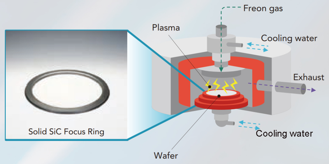
1. Plasma Etching Chamber and Focus Ring
Products: CVD SiC coated liners, showerheads, susceptors, and focus rings.
Application: In plasma etching, highly active plasma is used to selectively remove materials from wafers. Uncoated or less durable materials degrade rapidly, resulting in particle contamination and frequent downtime. CVD SiC coatings have excellent resistance to aggressive plasma chemicals (e.g., fluorine, chlorine, bromine plasmas), extend the life of key chamber components, and reduce particle generation, which directly increases wafer yield.
2.PECVD and HDPCVD chambers
Products: CVD SiC coated reaction chambers and electrodes.
Applications: Plasma enhanced chemical vapor deposition (PECVD) and high density plasma CVD (HDPCVD) are used to deposit thin films (e.g., dielectric layers, passivation layers). These processes also involve harsh plasma environments. CVD SiC coatings protect chamber walls and electrodes from erosion, ensuring consistent film quality and minimizing defects.
3. Ion implantation equipment
Products: CVD SiC coated beamline components (e.g., apertures, Faraday cups).
Applications: Ion implantation introduces dopant ions into semiconductor substrates. High-energy ion beams can cause sputtering and erosion of exposed components. The hardness and high purity of CVD SiC reduce particle generation from beamline components, preventing contamination of wafers during this critical doping step.
4. Epitaxial reactor components
Products: CVD SiC coated susceptors and gas distributors.
Applications: Epitaxial growth (EPI) involves growing highly ordered crystalline layers on a substrate at high temperatures. CVD SiC coated susceptors offer excellent thermal stability and chemical inertness at high temperatures, ensuring uniform heating and preventing contamination of the susceptor itself, which is critical to achieving high-quality epitaxial layers.
As chip geometries shrink and process demands intensify, the demand for high-quality CVD SiC coating suppliers and CVD coating manufacturers continues to grow.
IV. What are the challenges of CVD SiC coating process?
Despite the great advantages of CVD SiC coating, its manufacturing and application still face some process challenges. Solving these challenges is the key to achieving stable performance and cost-effectiveness.
Challenges:
1. Adhesion to substrate
SiC can be challenging to achieve strong and uniform adhesion to various substrate materials (e.g., graphite, silicon, ceramic) due to differences in thermal expansion coefficients and surface energy. Poor adhesion can lead to delamination during thermal cycling or mechanical stress.
Solutions:
Surface preparation: Meticulous cleaning and surface treatment (e.g., etching, plasma treatment) of the substrate to remove contaminants and create an optimal surface for bonding.
Interlayer: Deposit a thin and customized interlayer or buffer layer (e.g., pyrolytic carbon, TaC – similar to CVD TaC coating in specific applications) to mitigate thermal expansion mismatch and promote adhesion.
Optimize deposition parameters: Carefully control deposition temperature, pressure, and gas ratio to optimize the nucleation and growth of SiC films and promote strong interfacial bonding.
2. Film Stress and Cracking
During deposition or subsequent cooling, residual stresses may develop within SiC films, causing cracking or warping, especially on larger or complex geometries.
Solutions:
Temperature Control: Precisely control heating and cooling rates to minimize thermal shock and stress.
Gradient Coating: Use multilayer or gradient coating methods to gradually change material composition or structure to accommodate stress.
Post-Deposition Annealing: Anneal the coated parts to eliminate residual stress and improve film integrity.
3. Conformality and Uniformity on Complex Geometries
Depositing uniformly thick and conformal coatings on parts with complex shapes, high aspect ratios, or internal channels can be difficult due to limitations in precursor diffusion and reaction kinetics.
Solutions:
Reactor Design Optimization: Design CVD reactors with optimized gas flow dynamics and temperature uniformity to ensure uniform distribution of precursors.
Process Parameter Adjustment: Fine-tune deposition pressure, flow rate, and precursor concentration to enhance gas phase diffusion into complex features.
Multi-stage deposition: Use continuous deposition steps or rotating fixtures to ensure that all surfaces are adequately coated.
V. FAQ
Q1: What is the core difference between CVD SiC and PVD SiC in semiconductor applications?
A: CVD coatings are columnar crystal structures with a purity of >99.99%, suitable for plasma environments; PVD coatings are mostly amorphous/nanocrystalline with a purity of <99.9%, mainly used for decorative coatings.
Q2: What is the maximum temperature that the coating can withstand?
A: Short-term tolerance of 1650°C (such as annealing process), long-term use limit of 1450°C, exceeding this temperature will cause a phase transition from β-SiC to α-SiC.
Q3: Typical coating thickness range?
A: Semiconductor components are mostly 80-150μm, and aircraft engine EBC coatings can reach 300-500μm.
Q4: What are the key factors affecting cost?
A: Precursor purity (40%), equipment energy consumption (30%), yield loss (20%). The unit price of high-end coatings can reach $5,000/kg.
Q5: What are the major global suppliers?
A: Europe and the United States: CoorsTek, Mersen, Ionbond; Asia: Semixlab, Veteksemicon, Kallex (Taiwan), Scientech (Taiwan)
Post time: Jun-09-2025