SiC has the characteristics of large bandgap, high thermal conductivity, high critical breakdown field strength, and high electron saturation drift rate. It can meet the application requirements under high temperature, high pressure, high frequency, and high power conditions. It can be widely used in new energy vehicles, photovoltaics, industrial control, radio frequency communications and other fields. With the rapid development of related industries, the third-generation semiconductor market represented by silicon carbide has ushered in new opportunities.
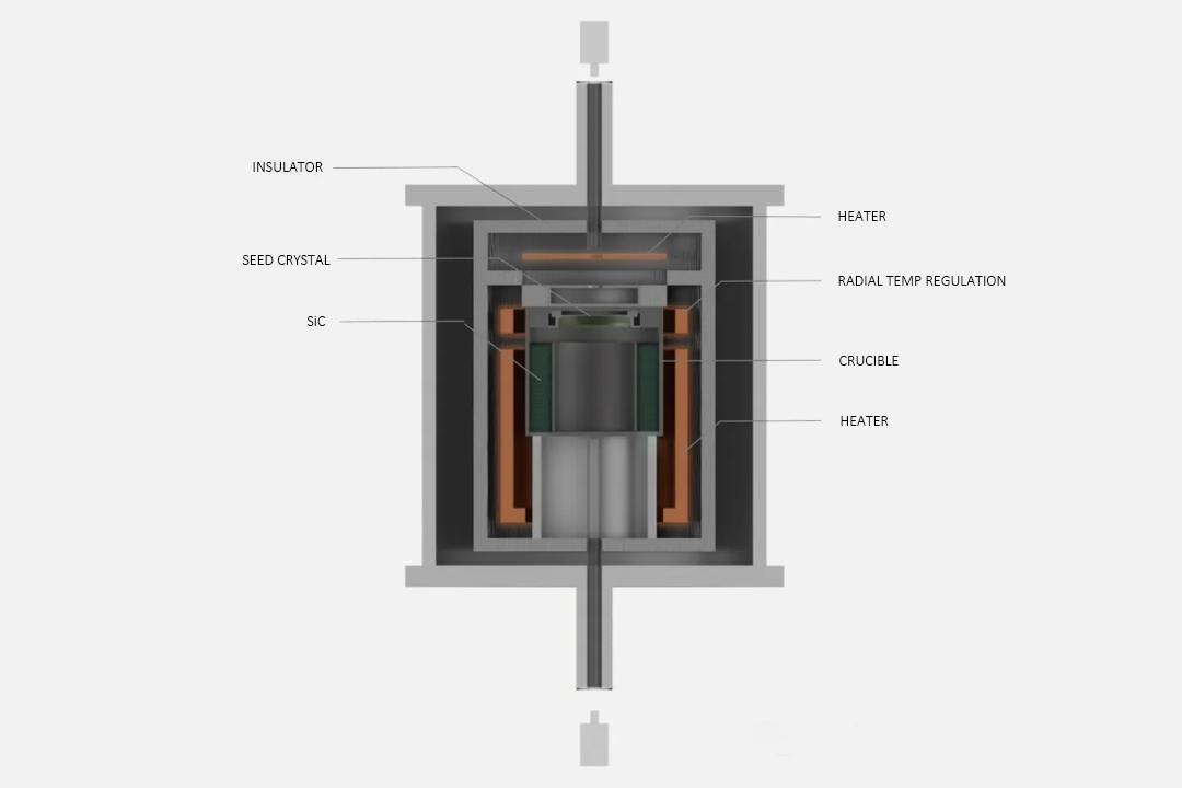
Crystal growth is the core link of silicon carbide substrate production, and the core equipment is the crystal growth furnace. Similar to traditional crystalline silicon-grade crystal growth furnaces, the furnace structure is not very complicated. It is mainly composed of furnace body, heating system, coil transmission mechanism, vacuum acquisition and measurement system, gas path system, cooling system, control system, etc. The thermal field and process conditions determine the key indicators of silicon carbide crystal quality, size, conductivity and other key indicators.
Ⅰ. Difficulties in silicon carbide crystal growth technology
The temperature of silicon carbide crystal growth is very high and cannot be monitored, so the main difficulty lies in the process itself:
(1) Difficulty in controlling the thermal field: The monitoring of the closed high-temperature cavity is difficult and uncontrollable. Unlike the traditional silicon-based solution-pulled crystal growth equipment, which has a high degree of automation and the crystal growth process can be observed, controlled and adjusted, silicon carbide crystals grow in a closed space in a high-temperature environment above 2,000°C, and the growth temperature needs to be precisely controlled during production, which makes temperature control difficult;
(2) Difficulty in controlling the crystal form: Micropipes, polymorphic inclusions, dislocations and other defects are prone to occur during the growth process, and they affect and evolve each other. Micropipes (MP) are through-type defects with a size of several microns to tens of microns, which are killer defects of devices. Silicon carbide single crystals include more than 200 different crystal forms, but only a few crystal structures (4H type) are the semiconductor materials required for production. Crystal form transformation is prone to occur during the growth process, resulting in polymorphic inclusion defects. Therefore, it is necessary to accurately control parameters such as silicon-carbon ratio, growth temperature gradient, crystal growth rate, and gas flow pressure.
In addition, there is a temperature gradient in the thermal field of silicon carbide single crystal growth, which leads to native internal stress and the resulting dislocations (basal plane dislocation BPD, screw dislocation TSD, edge dislocation TED) during the crystal growth process, thereby affecting the quality and performance of subsequent epitaxy and devices.
(3) Difficult doping control: The introduction of external impurities must be strictly controlled to obtain a conductive crystal with directional doping;
(4) Slow growth rate: The growth rate of silicon carbide is very slow. Traditional silicon materials only need 3 days to grow into a crystal rod, while silicon carbide crystal rods need 7 days. This leads to a naturally lower production efficiency of silicon carbide and very limited output.
On the other hand, the parameters of silicon carbide epitaxial growth are extremely demanding, including the airtightness of the equipment, the stability of the gas pressure in the reaction chamber, the precise control of the gas introduction time, the accuracy of the gas ratio, and the strict management of the deposition temperature. In particular, with the improvement of the device’s withstand voltage level, the difficulty of controlling the core parameters of the epitaxial wafer has increased significantly.
In addition, with the increase in the thickness of the epitaxial layer, how to control the uniformity of the resistivity and reduce the defect density while ensuring the thickness has become another major challenge. In the electrified control system, it is necessary to integrate high-precision sensors and actuators to ensure that various parameters can be accurately and stably regulated. At the same time, the optimization of the control algorithm is also crucial. It needs to be able to adjust the control strategy in real time according to the feedback signal to adapt to various changes in the silicon carbide epitaxial growth process.
Ⅱ. The main difficulties in the manufacture of silicon carbide substrates:
1. The growth temperature is above 2000℃, which is twice as high as that of silicon.
2. The thickness of the crystal rod is small during the crystal growth period, and a 2cm silicon carbide crystal rod grows in 7 days.
3. The crystal type requirements are high, and there are only a few single-crystal silicon carbide with crystal structures.
4. Cutting wear is high, and silicon carbide has extremely high hardness.
In summary, the expensive time cost and complex processing technology determine the high cost of silicon carbide substrates, which limits the application of silicon carbide.
III. Classification of crystal growth furnaces
According to different heating methods, crystal growth furnaces can be divided into induction type and resistance type. At present, most of the equipment on the market is induction type, which has the advantages of low cost, simple structure, convenient maintenance and high thermal efficiency. However, due to the electromagnetic induction effect, the axial temperature and radial temperature of induction heating are coupled, and it is impossible to take into account both the crystal growth speed and the crystal growth quality.
The resistance thermal field growth platform can accurately control the axial temperature and radial temperature respectively, which is conducive to the growth of large-size crystals and improves the crystal growth rate. It is one of the solutions for the future high-quality 8-inch silicon carbide crystal growth.
Comparison between induction method and resistance method:
| Induction method | Resistance method | |
| Working principle | Induction heating is a heat treatment method that uses the magnetic effect of electric current to create a relatively high density of induced current on the surface layer of the workpiece, quickly heats it to the austenite state, and then quickly cools it to obtain a martensitic structure. | Resistance heating uses the Joule heat generated by the current passing through the conductor as the heat source. It can be divided into two categories: indirect resistance heating (electric heating element or conductive medium) and direct resistance heating. |
| Temperature control | The induction method heats the internal magnetic field through the induction coil outside the crucible. The heating speed is fast, but the distance between the induction coil and the crucible is far, the radiation area is dispersed, and it is difficult to accurately control the heat generation of the crucible surface in the horizontal direction. | The resistance method sets a separate heater, which is close to the crucible. By adjusting the heater, the temperature of the crucible surface can be more accurately controlled. |
| Large-size crystal growth | When adding multiple heating coils to the induction method thermal field structure, the magnetic fields may cross-interfere with each other, resulting in the magnetic field and heat not being easily distributed according to the design purpose, affecting the heating effect and crystal growth. | It is easier to design a multi-stage independent control heating system for resistance heating crystal growth equipment, and the radial gradient of the equipment itself is small, which can meet the needs of large-size crystal growth. |
| Crystal growth cycle | Induction method crystal growth takes about 10 days, annealing takes 10-15 days, and the overall growth cycle is 20-25 days. | The crystal growth cycle is about 5-7 days, and it can be annealed automatically, and the temperature drops slowly after power failure. |
| Energy consumption | The energy consumption of the resistance method is 2-3 times higher than that of the induction method. | |
| Yield level | The yield of crystals grown by the resistance method crystal growth furnace is greatly improved compared with the induction method crystal growth furnace | |
Post time: Jun-24-2025